Researchers at the Korea Advanced Institute of Science & Technology (KAIST) have developed a groundbreaking diagnostic technique capable of detecting “hidden defects” in semiconductors with 1,000 times the sensitivity of existing methods. These defects, or electronic traps, are microscopic irregularities that obstruct electrical current, directly impacting the efficiency of devices like memory chips and solar cells. By mapping these traps with extreme precision, the new method allows engineers to address performance degradation at its source, potentially leading to more durable and cost-effective electronic components.
Semiconductors serve as the foundational material for nearly all modern electronics, but their performance is often hampered by invisible flaws. These electronic traps capture electrons and prevent them from moving freely through the material, resulting in energy leakage and reduced operational life. Until now, identifying these traps with high accuracy has been a significant challenge for the industry, often leading to increased development costs and longer testing cycles.
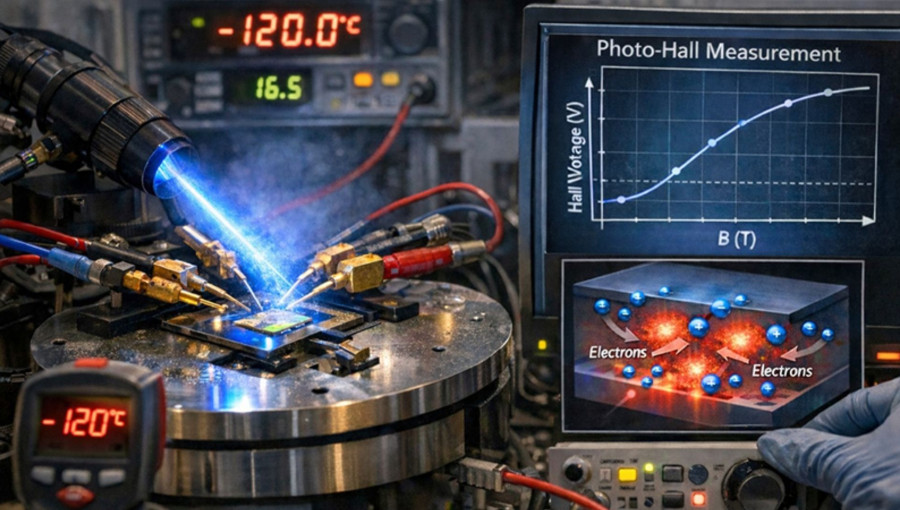
The research team, led by Professor Byungha Shin from the Department of Materials Science and Engineering at KAIST, overcame these limitations by enhancing traditional Hall measurements. This established technique typically uses electric and magnetic fields to study electron movement. However, the KAIST team introduced controlled light exposure and temperature variations to the process, allowing them to observe electrical behaviors that were previously undetectable.
During the testing process, the semiconductor is exposed to incremental intensities of light. At low levels, the newly generated electrons are absorbed by the internal traps. As the light intensity increases, these traps eventually become saturated, allowing additional electrons to move freely. By meticulously tracking these transitions, the researchers can calculate the exact number of traps present and the strength of their interaction with electrons.
A significant advantage of this new approach is its efficiency; it provides critical data on electron mobility, lifetime, and travel distance within a single experiment. The team validated the method using both standard silicon and perovskite materials, which are currently being explored for next-generation solar cells. In both instances, the technique identified extremely low concentrations of defects that conventional tools would have missed.
According to the study published in the journal Science Advances, this innovation is expected to become a vital tool for the semiconductor industry. By providing a deeper understanding of how defects interfere with electrical transport, the method enables the design of high-performance solar cells and memory chips with significantly improved reliability. This advancement not only promises better consumer electronics but also supports the transition to more efficient renewable energy technologies.